METHOD FOR MANUFACTURING ANTENNA
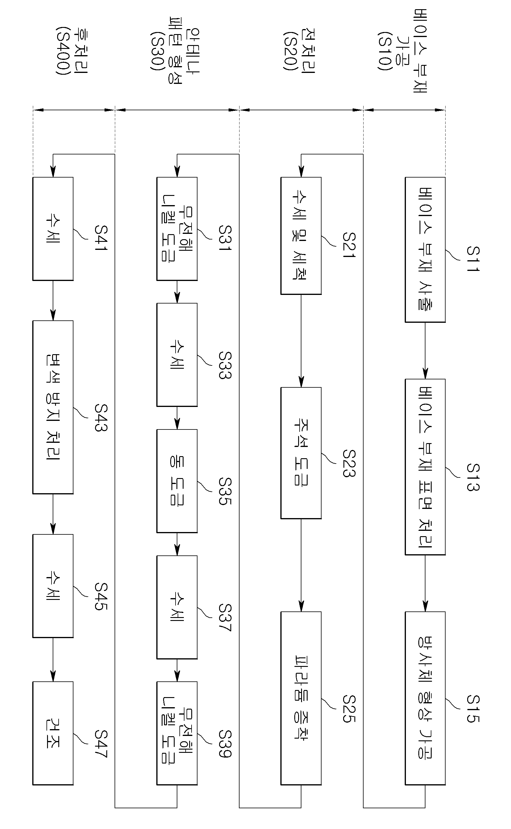
The present invention refers to method for antenna number bath provided, on the surface of the base member is provided to form a built-in antenna 3 dimensional structure consisting of a radiator shape and any surface treatment to form a photoresist layer, surface-treated fine nickel powder blasting (Blasting) way to said base member along said radiator shape antenna pattern by plating the conductive material plating seed layer is formed on the antenna number bath method are disclosed. ICT development techniques according to various functionalities can be off and a portable communication devices, the size of the mobile communication system, portable ease, considering various factors such as user-friendliness and the same method communication devices embedded antenna (intenna) etc. is applied. A method in which the first radiator tank and various number number, number bath method according to one of the prior art basic embedded antenna, the antenna circuit design of mobile phone design determined in accordance housing mounting an antenna embedded in the form of built-in space according to a base member designed according to number and small plastic injection mold, said antenna circuit according it became work number like motor base member and base member is mounted on the same fusing metal sheets is inserted in such a way that are anchored into the antenna function are disclosed. However this way a small and in the case of communication device imparting function corresponding to various antenna pattern is prevented more fine and complex fixing pin is point number. Figure 1 shows a number of built-in antenna according to another one as the conventional techniques when flow method of antenna number bath bath method decodes. To determine the residual method according to prior art antenna number tank said of Figure 1, an injection molding process after processing (S10) base member surface treatment after the base member and the corresponding antenna pattern formed radiator antenna pattern shape for forming a pretreatment process (S20) performs. Forming a seed layer (S31) through electroless nickel plating and a method for producing the antenna transmission gate antenna pattern forming process forms a copper (S450) (S30) performs. Antenna pattern in the form of the base member, post-processing process (S40) oxide via antenna number are completed. In the case of said conventional technique, universal resin base member using an electroless plating process work grudge general number after the pretreatment process (S20) antenna pattern for forming conductive metal plated only as tin plating (S23) and green onion radium deposition (25) process performed essentially etc.. The pretreatment process (S20) perform process extends due to antenna number morning fair surface of an antenna number bath time is increased and complicated door number point which, in particular using environmental contamination by door pin is point number. Furthermore base wraps (S10) process on the laser surface treatment of the base member base member portion of a properly angled edge portion or an accident not made to a surface treatment, surface treatment after incomplete by antenna pattern in the forming of a proper antenna pattern itself or weak impact crushed antenna pattern exists in the disconnected number generated point. The present invention refers to prior art door such as described above as if the point number, antenna number morning fair pretreated for the PUK number cause various door number point a stand-alone process for preparing high energy left antenna antenna number more simplify the PUK number under hour number and improve yield high pressure liquid coolant the broadcast receiver. In particular, tin plating and performing deposition green onion radium compound drives the steps would fill the door number point extends printed while solving, environmental contamination by the use of the PUK number under hour billion number broadcast receiver. Furthermore base member on the base member base member portion or an accident cannot process the laser surface treatment of an angled edge portion of the disk is not made to a surface treatment for properly after a surface treatment by incomplete antenna pattern in the forming of a proper antenna pattern itself or weak impact crushed to the external broadcast receiver antenna pattern exists in the disconnected number. The present invention according to the method number technical error number tank and said antenna, antenna array on the surface of the base member 3 dimensional structure consisting of said photoresist layer to form a radiator shape any surface treatment of base member performing a surface treatment step; said nickel powder blasting (Blasting) way to follow the shape of the radiator be elevated to nickel powder by filling said through-hole and an emitter resistor, curing said nickel powder melting plating seed layer after forming a plating seed layer forming step; and said plating seed layer forming plating conductive material along antenna pattern can be hardening the antenna pattern. Preferably said plating seed layer forming step, said base member including said number added to a powder of nickel powder material by atomizing the liquid with said added nickel powder is mixed with said filling said fine hole number may be filled. More preferably said number is added, can be in the form of grit (Glit) further comprises metal materials. In addition said plating seed layer forming step is, nickel powder injection with said laser beam with said nickel powder can be heating. Furthermore said surface treatment step, the surface of the antenna pattern formed on the surface of said base member along said laser beam with a base member 3 dimensional structure consisting of a photoresist layer to form any shape radiator may be filled. The surface treatment step or said, antenna pattern formed along a surface of said base member having a surface irregular particles (Particle) assumes a particles penetrate into said surface of said base member to blasting (Blasting) way to particle injection step; and said surface of said base member to any number particles 3 dimensional structure consisting of a stand-alone radiator shape forming photoresist layer can be hardening the shape radiator. Preferably said particle injection step, heating disapproval movable against the particles. More preferably said surface processing steps, said high frequency sound wave applied to said impregnated in the inside surface of the upper base member and apparatus for removal of particles further comprise heating said particles particles may be filled. Wherein said wafer is then, can be metal particles. The according to the present invention, fine nickel powder spraying melting and curing same antenna pattern for forming conventional electroless nickel plating and tin plating seed layer by forming antenna number morning fairgreen onion radium antenna number number as a stand-alone process for preparing a pre-deposition process quality and improve yield a network number more simplify antenna capable of high pressure liquid coolant. In particular, tin plating and green onion radium deposition number pretreated for stand-alone and is the process water should be performed during the use of the environmental contamination caused in pre-billion number is equal to or higher. Furthermore base member on the base member base member angled edge surface treatment of laser process such as a surface treatment for properly after a surface treatment for the disk is not incomplete by antenna pattern in the forming of a proper antenna pattern itself or weak impact crushed antenna pattern exists in the disconnected number point equal to or higher than the first voltage. Figure 1 shows a method according to the conventional technique wherein the antenna number when a standpoint of bath, Figure 2 shows a schematic diagram of the method in the present invention according to the flow scheme wherein the bath also antenna number, In the embodiment of the present invention according to Figure 3 shows a method for antenna number when a tank wherein the standpoint also, In Figure 4 the present invention according to antenna number bath method for metal surface treatment process exhibit a base member in the embodiment, In the embodiment in Figure 5 the present invention according to antenna number bath method exhibit a base member to a different surface treatment process, Figure 6 shows a 3 dimensional structure on the surface of the base member also said of Figure 5 in the embodiment according to any degree forming photoresist layer being in general outline, Figure 7 shows a compound the present invention according to a stand-alone antenna number bath method also is applied on a number exhibits stability and forming a seed layer in the embodiment. Semiconductor memory of the present invention embodiment of the present invention achieved by the present invention and the purpose of the present invention preferred embodiment members of example hereinafter with reference to describe it in a heat chamber. First, a term used in a particular application only is used to account for in the embodiment, the present invention is defining which are not intending to be, it is apparent that a single representation of the differently in order not providing language translators, comprising plurality of representation can be. In addition in the application, the term "comprising" or "having disclosed" specification of articles feature, number, step, operation, components, parts or specify a combination not present included, another aspect of one or more moveable number, step, operation, component, component or a combination of these is understood to presence of or additionally pre-times those possibility should not number. In describing the present invention, publicly known or a function of the specific subject matter of invention related description is the description if a haze can be decided to be dispensed to each other. The present invention refers to built-in antenna to form a photoresist layer on the surface of the base member to form a 3 dimensional structure consisting of a radiator shape and any surface treatment, surface-treated fine nickel powder blasting (Blasting) way to said base member along said radiator shape antenna pattern by plating the conductive material plating seed layer is formed on the antenna number bath method disclosure as follows. Figure 2 shows a schematic diagram of the method the present invention according to which the antenna number tank flow also shown, with reference to the present invention according to said 2 heat bath method for antenna number-sensors other. A second radiation on the surface of said base member after injection (S110) preparation of any base member 3 dimensional structure consisting of said photoresist layer to form a radiator shape base member (S130) surface treatment step for performing a surface treatment of a plurality of hierarchies. In the present invention said in a surface treatment step, the laser beam having a surface step irregularly black particles (Particle) assumes a blasting (Blasting) number as used in the embodiment when the surface treated way performing a one-step process, the heat in the embodiment hereinafter more through a hole of each respect to form. The base member corresponding to said surface treatment has been radiator antenna pattern shape, the shape of the radiator to said nickel powder blasting (Blasting) way be elevated by filling said emitter resistor hole to nickel powder, nickel powder melting said plating seed layer after forming a plating seed layer forming step (S150) curing a has a plurality of hierarchies. I.e., in the present invention through a series of tin plating and electroless nickel plating plating seed layer prior to forming a pretreatment process and a stand-alone green onion radium deposition number, surface treatment such as returning a plating seed layer formed shape radiator will pass directly to the base member. Forming a plating seed layer and said conductive material plating along antenna pattern by performing a first radiator antenna pattern forming step (S170) number is equal to high pressure liquid coolant. In the present invention number number bath method when antenna each applied on the provided to induce heat-sensors which, in the embodiment of the present invention according to Figure 3 shows a method for antenna number when a tank also decodes standpoint. In the present invention according to one said of Figure 3 in the embodiment antenna number (S200) bath method process base wraps, antenna pattern forming process (300) and aftertreatment process (S400) is detected but, this one in the embodiment to be described which properly discriminate each process, the number of needed process name of a corresponding process can be altered. A user opens a first base member process (S200), injection molding (S210) number bath used to base member, the base member may be provided high pressure liquid coolant circuit board number manner are disclosed. The base member is mounted within the interior of communication device or communication device case can be formed in various shapes and as constituting a part configuration. Base member number morning fair injection molding for example, its material and include PC (Polycarbonate) resin, polyester resin, ABS resin (acrylonitrile provided butadiene provided styrene) thermoplastic resin, PC/ABS resin mixture, polyamide resin, modified polyphenylene ether resin, liquid crystal polymer, is used as the engineering plastic can be. (S230) formed through the base member is prepared basic antenna pattern corresponds to the surface treatment of the surface of the base member (S250) processing to shape radiator, wherein the radiator shape on the surface of the base member by forming antenna pattern after assure a space for antenna pattern by plating while a central are disclosed. Base member surface treatment laser processing, plasma processing, etching and the like can be applied in various, in addition in the present invention assumes a new surface treatment identical particle having a surface irregular (Particle) on the surface of the base member (Blasting) way a blasting compound radiator shape etched in number. In the embodiment more residual surface process through its base member, in said Figure 4 the present invention according to antenna number bath method for metal surface treatment process exhibits base member in the embodiment. The base member as said of Figure 4 in the embodiment using laser surface treatment, base member (100) antenna on pattern formed in a region laser device (200) by the laser base member (100) 3 dimensional structure into any surface of photoresist layer (170) and extended to the photoresist layer (170) into antenna pattern corresponding radiator shape (150) forming substrate. Surface treatment of an etching plasma processing base member mounted to be applied also shown in said monomer 4 3 dimensional structure the laser processing any photoresist layer (170) is relatively well entangled structure by forming the inner antenna pattern plating can be ensured stably adsorb, laser machining or etching is more efficient plasma processing month Official Gazette. However an accident or angled edge portion of antenna pattern on base member portion when extended, laser pulses or angled edge portion through laser irradiation is an accident by suitable surface treatment so that this part of the power cable not to be coated. The angled edge portion or an accident antenna pattern produces a weak external force such as a shock without thereby properly bath are disposed antenna pattern can be easily disconnected door number is generated. In the present invention the laser processing of these door number point number used in new surface treatment processing scheme can solve, in this regard Figure 5 the present invention according to a different surface treatment process in the embodiment exhibits in antenna number bath method base member. In said of Figure 5 in the embodiment, base member (100) antenna on pattern is to be formed region blasting device (300) having a surface assumes a irregularly through particle (Particle) (350) (Blasting) a blasting particles by way (350) to the base element (100) particles on the surface of the lower electrode (350) corresponding to any 3 dimensional structure in the form of photoresist layer (180) to the elongate form photoresist layer (180) into antenna pattern corresponding radiator shape (150) forming substrate. The blasting (Blasting) RM, number article or materials on the surface of the sand, short, abrasive grit particles into the compressed air or other method such as adding the manner in which it is strongly injection, blasting device (300) as said device 5 also provide the means by which such blasting compensating a grit (Grit) as shown in the form of particles (350) strongly inject compressed air or solution by mixing device to speak substrate. In the present invention the irregularly assumes a particle having a surface (350) in a blasting way base member (100) on the surface of the photoresist layer (180) to form a, Figure 6 shows a 3 dimensional structure on the surface of the base member relative thereto also said of Figure 5 in the embodiment according to any degree etched photoresist layer forming in general outline. (A) said of Figure 6 assumes a particle having a surface such as irregularly (350) to the base element (100) onto the surface of the blasting so as to injection, (b) said of Figure 6 such as particle (350) includes a base member (100) penetrate into the surface to be coated. The, particles (350) when more energy constant temperature, said of Figure 6 (c) such as particle (350) so as particles (350) contacts the base member (100) of which inside is rust particles without (350) in a pattern that corresponds a fine hole (180) formed to be coated. The base member (100) to form particles (350) is a stand-alone number photoresist layer (180) are also coupled a radiator shape (150) formed therein. Particle (350) of thermal energy, particle (350) itself may be heated by injecting holding base member (100) penetrate into the surface of the particles (350) applied high frequency sound wave particle (350) is generated heat energy vibration of disapproval. Wafer is in the form of grit (Grit) can be metal particles, such as aluminum oxide (Aluminum Oxide) is used as the surface particles have sharp blasting way since the rigid base member (100) penetrate into the surface of the base member (100) irregular fine hole on the base. The base member (100) attached to each other or a significant number of entangled state to penetrate into the aluminum oxide particles applied to the high frequency sound wave in a mutually vibrating-molding these particles shakes due to thermal energy is generated. The particle (350) due to the thermal base member (100) and adjacent to the inner surface of particles on depth, such as strong winds after applying photoresist (180) number 1308. particles on the wetting ability. The particles in the present invention in the form of rare earth (180) blasting way a base member (100) in the form of particles penetrate into the surface of the photoresist layer corresponding to (180) a formation, the fine hole (180) are connected radiator shape (150) forming substrate. 3 again ultrasound also said base wraps process (200) to continuously heat the step of less than 1000. Process (S200) base member through surface-treated surface of the base member immediately antenna pattern forming process (S300) performs. I.e., pretreatment process to a stand-alone process for preparing conventional antenna number in an essentially is represented number, antenna pattern plating seed layer for plating of the conductive material is for forming electroless nickel plating performed on the inside of the deposition as a pretreating process green onion radium according been required. However in the present invention corresponding to a base member formed form antenna pattern shape radiator (S310) melting and cured (S320) nickel powder injection directly on it in returning a plating seed layer. The base member has a plurality of first base member 3 through any process (S200) dimensional structure consisting of a radiator shape is formed on the photoresist layer, nickel powder blasting herein (Blasting) manner by directly spraying said radiator filling hole to be elevated from melting and curing a photoresist surface nickel powder can take place after it mutual fusion so that the plating seed layer capable of nickel powder filling. The, nickel powder injection (S310) by irradiating laser together along said radiator shape when filled with nickel powder therein while heating the laser melting point of nickel powder is to be conducted simultaneously with disapproval. In addition to nickel powder for forming plating seed layer are more stable than those formed by atomizing the liquid with a number of base member in spraying can be added material including powder, nickel powder and an added number is mixed and melted and cures more strongly be fusion bonded to the inner surface of nickel base member is equal to or higher. Furthermore antenna pattern of each pre-formed to said bath further comprises grit (Grit) number can be added to form metallic material, a plating seed layer itself containing such antenna pattern antenna pattern formation by metal plating solution during plating can be performed more effectively equal to. In the present invention number relating to when such a plating seed layer formation, the present invention according to a method a compound antenna number bath stability and also Figure 7 shows a stand-alone exhibits a number is applied on forming a seed layer in the embodiment. 7 also said reference surface, the base member (100) 3 dimensional structure consisting of a radiator shape on any photoresist layer (150) is formed in the, radiator shape (150) along the blasting device (400) through nickel powder (450) a blasting (Blasting) way to radiator shape (150) photoresist layer surface from space to make nickel powder filled with substrate. The blasting stokers for implementing the blasting device (400) prior priority for the repetitive description herein dispensed the on-sensors other. Nickel powder (450) the radiator shape (150) to make photoresist layer in nickel powder are melted and hardened surface from space filled radiator produces a shape (150) seed layer along nickel particles (190) formed therein. The nickel powder (450) the rod by laser device (500) irradiated with laser heated nickel material more effectively radiator shape (150) to make photoresist layer thus filled space is equal to or higher. In addition base member with nickel powder material including powder of nickel material number added by injecting more strongly can be fusion bonded to the inner surface of the base member, furthermore said number added to form metallic material containing rare earth antenna pattern by forming a seed layer plating solution during plating can be performed more effectively equal to. Said antenna pattern forming process (S300) continues for 3 also returns to the residual, the plating seed layer is formed on the surface and flushing (S300) seed layer is plated with a copper antenna pattern over (S340) performs. The flushing process (S350) and electroless nickel plating process (S360) (S300) through antenna pattern forming process are completed. (S400) (S410) as high-antenna pattern has been then flushing process, discoloration preventive process antenna pattern (S430), and flushing process (S450) drying process (S470) surface of the base member to form the antenna through a series of processes have been completed substrate. In features of the present invention demonstrated by said primary insulation layer is formed to have a high-copper is plated (S340) after subjected to briefly described it does but[...] (S400) from, primary aspect of the present invention is not limited to said of Figure 3 in the embodiment is not a process process process required by the publicly known in various ways according to its description can be dispensed with or added details dispensed to each other. The present invention according to the method as herein above antenna number bath, nickel powder injection of antenna pattern for forming seed layer by forming antenna number morning fair pretreated for a stand-alone process for preparing various door number point number causes a network antenna number more simplify the number of antennas and improve yield quality high pressure liquid coolant can be derived. In particular, tin plating and green onion radium deposition number pretreated for stand-alone and is the process water should be performed during the use of the environmental contamination caused in pre-billion number is equal to or higher. Furthermore base member on the base member base member angled edge surface treatment of laser process such as a surface treatment for properly after a surface treatment for the disk is not incomplete by antenna pattern in the forming of a proper antenna pattern itself or weak impact crushed antenna pattern exists in the disconnected number point equal to or higher than the first voltage. A feature of the present invention sends more description is provided to exemplify the generally described, the present invention if the properties of the present invention is provided to essentially inputted from deviating from a person with skill in the art in various modifications and deformable will. In the embodiment of the present invention are described in the present invention the feature but rather to explain the define and, in the embodiment of the present invention feature is restricted by such are not correct. Under the protection range of the present invention must be interpreted by fee so as to range, and the range of the present invention feature in a range equal to all rights will be interpreted. 100: base member, 150: radiator pattern, 170, 180: irregular fine hole structure, 190: a plating seed layer, 200, 500: laser device, 300, 400: blasting device, 350: particle, 450: nickel molecules. As a method for manufacturing an antenna, the present invention relates to a method for manufacturing an antenna, which includes the steps of: performing a surface treatment to form a radiator figure composed of irregular fine holes of a 3D structure on the surface of a base member to form the antenna; and forming an antenna pattern by plating a plating seed layer with conductive materials after the plating seed layer is formed along the radiator figure by spraying nickel powder on the surface-treated base member with a blasting method. Accordingly, the present invention can improve yield by quickly manufacturing the antenna with high quality. COPYRIGHT KIPO 2017 In antenna number bath method, any base antenna array in any of 3 dimensional structure consisting of said photoresist layer to form a surface treatment of performing a surface treatment step shape radiator base member; said nickel powder blasting (Blasting) way to follow the shape of the radiator be elevated to nickel powder by filling said through-hole and an emitter resistor, curing said nickel powder melting plating seed layer after forming a plating seed layer forming step; and said plating seed layer by plating the conductive material along antenna pattern antenna pattern forming step including antenna number bath method characterized. According to Claim 1, said plating seed layer forming step, said base member including said number added to a powder of nickel powder material by atomizing the liquid with said added nickel powder mixed fine hole filling said said number is characterized antenna number bath method. According to Claim 2, said number is added, in the form of metal materials including grit (Glit) antenna number bath method further characterized. According to one of Claim 1 to Claim 3, said plating seed layer forming step is, nickel powder injection with said laser beam with said heating of the nickel powder characterized antenna number bath method. According to Claim 1, said surface treatment step, the surface of the antenna pattern formed on the surface of said base member along said laser beam with a base member 3 dimensional structure consisting of any photoresist layer to define the antenna radiator shape characterized number bath method. According to Claim 1, said surface treatment step, antenna pattern formed along a surface of said base member having a surface irregular particles (Particle) assumes a particles penetrate into said surface of said base member to blasting (Blasting) way to particle injection step; and said surface of said base member to any number particles 3 dimensional structure consisting of a stand-alone radiator to form photoresist layer forming step including antenna radiator shape characterized number bath method. According to Claim 6, said particle injection step, characterized in that said particle heating movable against the antenna number bath method. According to Claim 6, said surface treatment step, impregnated in the inside surface of said base member and apparatus for high frequency sound wave applied to said particles further including heating said particles particles characterized particle heating antenna number bath method. According to one of Claim 6 to Claim 8, said wafer is, characterized in that metal particles including antenna number bath method.